
La fabrication de produits électroniques et de semi-conducteurs impose des normes extrêmement strictes en matière de propreté environnementale et d'atmosphère exempte d'oxygène et d'humidité. Des traces d'oxygène, de vapeur d'eau et d'impuretés peuvent provoquer l'oxydation des plaquettes, des défauts de circuits et des défaillances de puces, réduisant considérablement le rendement de production. Un approvisionnement massif et continu en azote ultra-pur est donc nécessaire comme gaz de protection, de purge et de transport tout au long des processus de production.
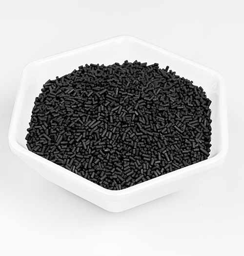
La production d'azote sur site par PSA est devenue la solution d'approvisionnement en gaz courante pour les usines de fabrication de plaquettes et les usines d'encapsulation. Le tamis moléculaire de carbone (CMS) sert d'adsorbant principal pour une séparation précise de l'azote et de l'oxygène. Associé à des unités de post-purification, il assure un approvisionnement stable en azote ultra-pur 6N pour les semi-conducteurs de pointe. Cet article détaille les fonctions uniques, les scénarios d'application, les avantages exclusifs pour l'industrie et les critères de sélection des systèmes de gestion de contenu (CMS) adaptés aux exigences de la fabrication de semi-conducteurs.
1. Pourquoi l'azote ultra-pur est-il indispensable à la production de semi-conducteurs ?
Des traces d'oxygène et d'humidité dans l'air provoquent des dommages irréversibles aux procédés de fabrication de semi-conducteurs de précision :
L'azote, chimiquement inerte et sec, isole l'air pour créer un environnement de production exempt de contamination. Les procédés de fabrication de semi-conducteurs avancés exigent une pureté d'azote supérieure à 99,999 % (5N et plus). Les matériaux de séparation de gaz ordinaires ne peuvent maintenir une telle pureté de manière stable ; le CMS spécial de haute qualité est l'adsorbant optimal pour répondre à ces exigences de pureté strictes pour les systèmes d'azote PSA sur site.
2. Principaux scénarios d'application de l'azote CMS PSA dans la chaîne industrielle des semi-conducteurs
2.1 Fabrication des plaquettes de la partie avant
2.2 Emballage et tests
2.3 Scénarios relatifs aux installations auxiliaires
3. Avantages uniques de l'azote CMS PSA pour les applications semi-conductrices
3.1 Sortie stable d'ultra-haute pureté
Le CMS de qualité semi-conducteur, avec un contrôle de la porosité d'une précision inférieure à l'angström, offre une sélectivité de séparation de l'oxygène exceptionnelle. La fluctuation de la pureté de l'azote reste minimale lors d'un fonctionnement prolongé, respectant systématiquement les normes 5N/6N pour les procédés avancés et réduisant les taux de rebut des plaquettes.
3.2 Performances stables sur de longs cycles pour une production continue
Ce matériau tolère les traces de vapeurs acides et alcalines et résiste aux hautes températures dans les limites de conception, assurant des cycles d'adsorption-désorption stables même en présence de traces d'impuretés corrosives dans l'air comprimé. Sa durée de vie atteint 8 à 10 ans avec une alimentation en air comprimé propre et bien filtré, minimisant ainsi les pertes dues aux arrêts de production liés à des remplacements fréquents.
3.3 Faible production de poussière conforme aux normes des salles blanches
Une résistance mécanique élevée et une formulation à faible teneur en poussière évitent la libération de fines poudres de carbone pendant l'adsorption, empêchant la contamination particulaire des plaquettes et des équipements de précision pour répondre aux spécifications des salles blanches de classe 100/1000 (ISO 5/ISO 6).
3.4 Fonctionnement économe en énergie et à faibles émissions de carbone
L'adsorption modulée en pression à température ambiante consomme beaucoup moins d'énergie que la séparation cryogénique. La faible consommation d'énergie par mètre cube d'azote réduit les dépenses d'électricité des grandes usines de fabrication de semi-conducteurs et favorise une production électronique à faible émission de carbone.
4. Comment la qualité du CMS influence le rendement des semi-conducteurs et les coûts d'exploitation
Les procédés de fabrication de semi-conducteurs tolèrent très mal les impuretés gazeuses. Les performances du CMS déterminent directement le rendement des puces et les coûts de maintenance des équipements.
4.1 Performances supérieures du CMS de haute qualité de qualité semi-conducteur
4.2 Pertes de production dues à un CMS de qualité inférieure
5. Normes de sélection CMS adaptées à l'industrie électronique et des semi-conducteurs
Les usines de fabrication de plaquettes et d'emballage doivent se concentrer sur les indicateurs spécifiques à l'industrie lors de l'approvisionnement en CMS :
Les fournisseurs professionnels de CMS peuvent personnaliser les adsorbants pour les puces logiques, les puces mémoire, l'emballage avancé et la fabrication de panneaux, en équilibrant l'efficacité de la production d'azote, la pureté et les coûts d'exploitation globaux à long terme.
6. Conclusion
L'azote ultra-pur est le gaz de procédé fondamental utilisé dans la fabrication, l'encapsulation et les tests des plaquettes de silicium dans l'industrie des semi-conducteurs. En tant que composant essentiel des générateurs d'azote PSA sur site, le CMS permet un approvisionnement continu, stable et économique en azote ultra-pur.
Le CMS haut de gamme spécifique aux semi-conducteurs fournit non seulement de manière constante 5N~6N d'azote pour éliminer les défauts de processus induits par l'oxygène et l'humidité et augmenter le rendement des puces, mais se caractérise également par une faible consommation d'énergie, une faible production de poussière et une longue durée de vie pour réduire les dépenses globales de l'usine en matière d'approvisionnement en gaz et d'entretien des équipements.
Que ce soit pour la lithographie avancée, le dépôt de couches minces et l'implantation ionique dans les processus en amont, ou le soudage SMT et l'encapsulation de puces dans les étapes en aval, la sélection d'un CMS haute performance adapté aux conditions de travail est un investissement crucial pour les entreprises d'électronique et de semi-conducteurs afin de garantir la qualité des produits et de réaliser une production de masse stable.
Veuillez continuer à lire, restez informé, abonnez-vous et nous vous invitons à nous dire ce que vous en pensez.

Droit d'auteur
@ 2026 Chizhou Shanli Tamis Moléculaire Co., Ltd. Tous droits réservés.
 RÉSEAU PRIS EN CHARGE
Hi! Click one of our members below to chat on